HQ Team
November 17, 2022: Scientists from the US Department of Energy’s Ames National Laboratory have developed a new “characterization tool” that may help to find an alternative to silicon in solar cells.
The scientists first developed a microscope that uses terahertz waves to collect data on material samples. The team then used their microscope to explore Methylammonium Lead Iodide (MAPbI3), a perovskite material.
Perovskites are semiconductors that transport an electric charge when exposed to visible light. The main challenge in MAPbI3 solar cells is that it degrades fast when exposed to elements like heat and moisture.
Characterization in materials science refers to a broad and general process by which a material’s structure and properties are probed and measured. Without the process, one cannot ascertain the scientific understanding of engineering materials.
Perovskite consists of calcium titanium oxide. Gustav Rose first discovered it in the Ural mountains of Russia in 1839, and it is named after Russian mineralogist L.A. Perovskite.
Thin-film technique
Synthetic perovskites are inexpensive base materials for high-efficiency commercial photovoltaics. They can be made using the same thin-film manufacturing techniques as that used for thin-film silicon solar cells.
Using the new microscope, the team of scientists at Ames investigated MAPbI3, which is of recent interest to scientists as an alternative to silicon in solar cells.
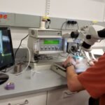
Led by Jigang Wang, a senior scientist from Ames Lab, the new scanning probe microscope used the terahertz range of electromagnetic frequencies to collect data on materials.
The terahertz range is far below the visible light spectrum, falling between the infrared and microwave frequencies. Then they shined the terahertz light through a sharp metallic tip, enhancing the microscope’s capabilities toward nanometer-length scales.
20-nanometer radius
“Normally, if you have a light wave, you cannot see things smaller than the wavelength of the light you’re using,” said Richard Kim, a scientist from Ames Lab.
“And for this terahertz light, the wavelength is about a millimetre, so it’s quite large. But here we used this sharp metallic tip with an apex that is sharpened to a 20-nanometer radius curvature, and this acts as our antenna to see things smaller than the wavelength we were using.”
The team expected MAPbI3 to behave like an insulator when exposed to the terahertz light.
Since the data collected on a sample is a reading of how the light scatters when exposed to the terahertz waves, the scientists expected a consistently low level of light disperses throughout the material.
“What they found, however, was that there was a lot of variation in light scattering along the boundary between the grains,” according to a statement on EurekAlert.
Light scattering
Conductive materials, like metals, would have a high level of light scattering, while less-conductive materials, like insulators, would not have as much. “The wide variation of light scattering detected along the grain boundaries in MAPbI3 sheds light on the material’s degradation problem,” Kim said.
The data collected on the material showed the degradation process through changes in the levels of light scatterings. “This information can be useful for improving and manipulating the material in the future,” Kim said.
Wang said the study demonstrated “a powerful microscopy tool to visualize, understand and potentially mitigate grain boundary degradation, defect traps, and materials degradation.”
“Better understanding of these issues may enable developing highly efficient perovskite-based photovoltaic devices for many years to come.”